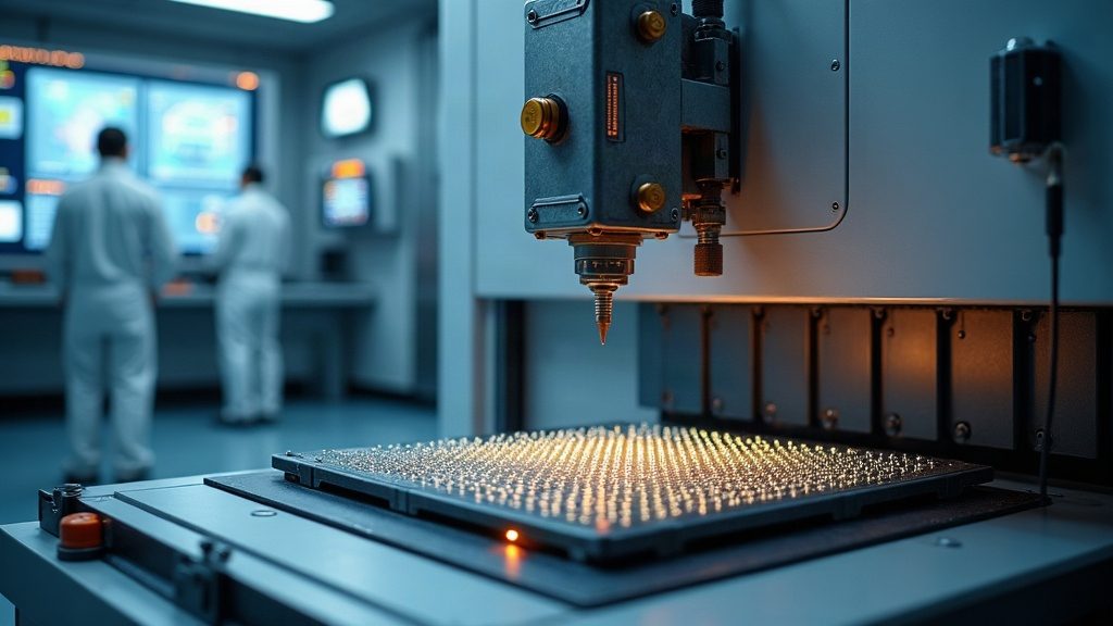
Samsung Opens AI Chip Packaging Center in Yokohama
The memory maker wants closer ties to Japan's adhesive, substrate and packaging-tool suppliers. Size, staffing and cost stay undisclosed.
In short
Samsung opened a research center for AI chip packaging in Yokohama on September 8, 2026, in order to work more closely with the Japanese suppliers that dominate the back end of chipmaking.
At a glance
- Opening: Tuesday, September 8, 2026, in Yokohama, Japan.
- Focus: advanced packaging, the assembly of AI chips after wafer fabrication.
- Collaboration target: Japanese makers of adhesives, substrates and assembly equipment.
- Funding: built with Japanese state support according to Nikkei Asia, with no amount given.
- Not on the record: investment size, floor space, headcount and the names of the supplier partners.
Samsung Electronics has opened a research center in Yokohama devoted to packaging AI chips. Nikkei Asia reported the move on September 9, 2026; the opening itself took place on Tuesday, September 8. The stated purpose is tighter coordination with the Japanese firms that shape the back end of chip manufacturing.
Why the back end decides AI performance
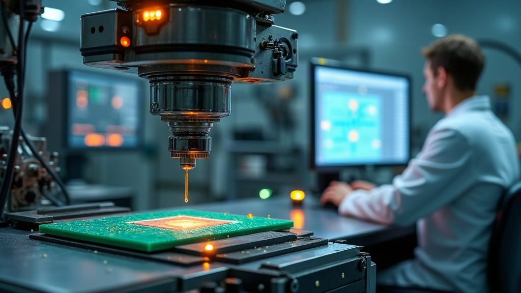
Packaging is what happens after the wafer is done: dies get stacked, wired together and mounted on a carrier. For AI accelerators, that stage governs how fast compute and memory can talk to each other. Progress there comes less from shrinking transistors than from better interconnects, adhesives and bonding tools.
The Japanese piece of the supply chain
The report identifies adhesives, substrates and assembly equipment as the areas Samsung wants to tap. Japan is unusually deep in exactly that layer of the supply chain, so sitting next to those vendors can shorten development cycles. A Yokohama address puts Samsung engineers within a short train ride of the people who make the materials.
What the accessible report does not establish
The freely readable portion of the Nikkei article stops after the opening paragraph. Nothing there supports a figure for investment, floor space, headcount or the identity of the partner firms. The standfirst points to Japanese state assistance without quantifying it. Jun Young-hyun is named as attending the opening, but the readable text gives no job title.
The open question
What matters next is whether the site houses its own engineering staff and lab equipment or functions mainly as a liaison office to the supplier base. The report is compatible with either. A Samsung press release or Japanese ministry documentation on the subsidy would be the places to settle it.
FAQ
Where is Samsung's new chip packaging research center?
In Yokohama, Japan. It opened on September 8, 2026.
What is advanced packaging in AI chips?
It is the stage after wafer fabrication in which several dies are stacked, interconnected and mounted on a carrier. It shapes how fast compute and memory exchange data.
How much is Samsung investing in the Yokohama site?
That is unknown. The accessible portion of the Nikkei report gives neither an investment figure nor the size of the Japanese state support it mentions.